#PHY with PIPE Interfac
Explore tagged Tumblr posts
Visit Tumblr Blog
Explore Tumblr blogs with no restrictions, modern design and the best experience.
Last Seen Tumblr Blogs


Fun Fact
China blocked Tumblr because of pornography and censorship problems in 2013.
Text
SERDES Interface- PHY with PIPE Interface-ASIC/SoC Physical Design-SoCs for Edge Computing
PHY with PIPE interface Multi-chipset designs execute ASICs and other incorporated items across various bites the dust inside a solitary bundle. The ODSA bunch expects to characterize an open consistent connection point to such an extent that chiplets from different sellers can be created to shape space explicit gas pedals. As a piece of this work, the ODSA studied and investigated a wide scope of new between chipset PHY advancements. This paper reports the aftereffects of the overview. We foster a system to assess these PHY advancements. In view of our investigation, we propose the utilization of a deliberation layer with the goal that numerous PHY innovations can introduce a typical connection point. Fringe Component Interconnect (PCI) Express is a cutting edge, elite execution, highlight point, broadly useful info yield interconnect correspondence convention. PCI Express overrides other heritage transports and gives higher data transmission which settles on it an optimal decision for some applications. It gives a layered design that contains three separate layers. Multichiplet framework in-bundle designs certainly stand out as an instrument to battle high SoC configuration costs and to monetarily fabricate huge ASICs. These designs require low-power region effective off-pass on-bundle pass on to-pass on correspondence. Current innovations either stretch out on-pass on high-wire count transports utilizing silicon interposers or off-bundle sequential transports. The previous methodology prompts costly bundling. The last option prompts perplexing and high-power designs. We propose a straightforward bundle of-wires interface that joins simplicity of advancement with minimal expense bundling methods. We foster the point of interaction and show how it tends to be utilized in multi chipset frameworks. The RTL of PCI Express Gen5.0 is planned in SystemVerilog language and for the check reason, the approach utilized is Universal Verification Methodology. Reproduction results show the adequacy of the proposed methodology which is displayed in the Synopsys Discovery Visual Environment apparatus effectively.
serialize-and-deserialize (SerDes) fast information grouping. The generally utilized current-mode rationale (CML) designs of hook and multiplexer/demultiplexer (MUX/DEMUX) are supplanted by the proposed TC way to deal with permit more headroom and to bring down the power utilization. Through the stacked transformer, the information clock pulls down the differential source voltage of the TC lock and the TC multiplexer center while switching back and forth between the two-stage tasks. With the upgraded channel source voltage, the TC configuration draws in more channel current with a less width-to-length proportion of NMOS than that of the CML partner. The source-offset voltage is diminished so the stock voltage can be decreased. The lower supply voltage further develops the power utilization and works with the joining with the low voltage supply SerDes interface. The MUX and the DEMUX chips are created in a 65-nm standard CMOS process and work at 0.7-V stock voltage. One potential arrangement distinguished is the sequential connection point, likewise named as SERDES (Serializer/DESerializer) interface. A run-of-the-mill SERDES interface contains encoder/decoder, PLL, timing-control, and multiplexer/de-multiplexer. Encoding of sequential information tackles rapid sequential information transmission issues by consolidating clock installing, DC adjusting, sync data addition, and mistake recognition. DC adjusting additionally addresses the issue of Inter-Symbol Interference (ISI). Accessible SERDES interface gadgets have constraints like unfortunate decrease factor, no clock inserting, or non-accessibility of the space-qualified parts. Thus, an endeavor is made to comprehend and carry out this connection point with the objective of native SERDES ASIC advancement, which will likewise defeat the above issues. Different sequential encoding methods are reviewed and an 8B/10B encoding procedure is finished for exceptionally rapid sequential information transmission. As an underlying advance, an 8B/10B encoding-based SERDES connection point is executed in an FPGA.
ASIC/SoC Physical Design A superior ASIC/SOC plan procedure for fast plan intermingling is portrayed in this paper. Dissimilar to the regular ASIC/SOC plan systems zeroed in on mechanization, our new technique centers around smoothing out the ASIC/SOC stream's planning-consuming strides by applying our master's BKMs to speed up plan combination. It empowered us to abbreviate the tedious stages significantly with moderately negligible exertion. This paper depicts the philosophy utilized by the IBM Microelectronics Division for the plan of its Blue Logic® application-explicit coordinated circuits (ASICs) and framework on-a-chip (SoC) plans. This philosophy is utilized by both IBM ASIC and SoC originators, as well as OEM clients. A critical focal point of the IBM ASIC/SoC approach, laid out in the primary part of this paper, is the initial time-right techniques for planning and checking that augment the right activity of the chip upon item combination. The second part of this paper portrays progress in an approach that arrangement with the actual impacts of contracting gadget calculations and empower configuration utilizing the exhibition and thickness abilities accessible in the new innovations, and strategic advances that have further developed plan completion time (TAT) for huge, complex plans. One variable for this development is that wire delays are expanding as a level of generally process duration. Thus, arrangement necessities to think about something beyond the productivity of the last plan. The position is presently a significant supporter of timing conclusion results. The issue space for the position currently covers a wide scope of configuration styles, including ASIC, SOC, and Microprocessor. Each of these acquaints remarkable difficulties with arrangement calculations. Likewise, the capacity of the situation calculations to work steadily inside a planning conclusion framework is developing inconsequentiality. -
0 notes
Text
PCIe 5.0 SerDes PHY Controller IP Cores For All High-End Serial Connect Interfaces In Advanced SoCs
T2MIP, the global independent semiconductor IP Cores provider & Technology experts, is pleased to announce the immediate availability of its partner’s PCI-SIG compliant PCIe 5.0 Serdes PHY IP Cores in 12FFC process nodes with matching PCIe 5.0 Controller IP Core which are silicon proven with High bandwidth and superfast data transfer speed.
The PCIe 5.0 PHY and Controller IP cores supports the PCI 5.0 Specification, compliant with PIPE 5.1. The structured yet simple design allows easy adoption into any design architecture. Lower power consumption is achieved due to support of additional PLL control, reference clock control, and embedded power gating control. The PHY and Link Layer comes with backward compatibility support for parallel interface: 16/32- bit (Gen5/4), 10/20-bit (Gen3/2/1).
The PCIe SerDes PHY and Digital Controller IP Cores provides minimal latency and superfast isochronous data transfer. The PCIe 5.0 SerDes PHY IP Core in 12nm FFC process technology supports varied data transfer rates of 2.5 GT/s, 5.0 GT/s, 8.0 GT/s, 16.0 GT/s and 32GT/s with four (x4) physical lane width.
The 12FFC technology comes with added feature of built-in EYE-monitor and EYE checker, dual-port PLL with LC tanks and a 3-tap FFE for TX preset. Gated power for lowest leakage in L1.2 low power mode, Auto power saving for short reach and Configurable low power mode setting makes the PHY widely applicable for various scenarios under different consideration of power consumption with an Operating Voltage of 0.8V and 1.2V.
PCIe 5.0 Controller IP Core provides full PCIE Controller functionality with Root Complex and Endpoint BFM modes. It supports queuing for 8 configurable Virtual Channels and multi-function Configurable TC to VC queue mapping. Speed and Link Width negotiation, polarity inversion, and lane-to-lane skew Configurable timers and timeouts allows for high controllability and Scaled Flow Control. Emergency Power Reduction State allows for an advanced power management system.
These IP Cores functionalities are verified in NC-Verilog simulation software using test bench written in Verilog HDL, which are provided with the IP Core delivery. The PCIe 5.0 SerDes PHY IP core along with the PCIe 5.0 Controller IP core have been used in semiconductor industry’s Enterprise computing, storage area networks, Wireless and mobile devices, automotive, IoT, Embedded systems, Graphics devices and other industrial uses…
In addition to PCIe IP Cores, T2M‘s broad silicon Interface IP Core Portfolio includes other USB, HDMI, Display Port, MIPI (CSI, DSI, UniPro, UFS, Soundwire, I3C), DDR, 10/100/1000 Ethernet, V by One, programmable SerDes, SD/eMMCs and many more, available in major Fabs in process geometries as small as 7nm. They can also be ported to other foundries and leading-edge processes nodes on request.
3 notes
·
View notes
Text
USB 3.0 PHY IP in 14SF+
For auxiliary devices, a Universal Serial Bus (USB) transceiver is offered. The PHY complies with the UTMI, USB 2.0 PIPE, and USB 3.0 (USB SuperSpeed) requirements. The USB3.0 PHY IP transceiver is designed to consume little power and take up little space on the chip without compromising speed or data throughput. The USB3.0 PHY IP includes a full on-chip physical transceiver solution with Electrostatic Discharge (ESD) protection, a built-in self-test module with inbuilt jitter injection, and a dynamic equalization circuit to ensure full support for high-performance designs. Multiple IP sources are supported by the USB3 MAC layer over the shared PHY interface (PIPE). Internal test monitoring and permitted modification of analogue circuit parameters Using consistent power, built-in Self-Test, integrated Jitter Injection Output and jitter is minimised.

1 note
·
View note
Text
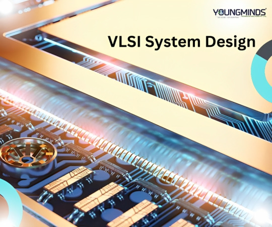
YoungMinds - VLSI System Design and It’s Importance
Full-form of VLSI is Very Large-Scale Integration, is the process of creating an integrated circuits (IC’s) by combining millions or billions of MOS transistors onto a single chip.
VLSI began in the 1970s when MOS integrated circuit (Metal Oxide Semiconductor) chips were developed and then widely adopted, enabling complex semiconductor and telecommunication technologies. The microprocessor and memory chips are VLSI devices.
VLSI is one of the most widely used technologies for microchip processors, integrated circuits (IC) and component designing. It was initially designed to support hundreds of thousands of transistor gates on a microchip which, as of 2012, exceeded several billion.
In VLSI, the programming languages for IC design are called hardware description languages (HDLs). These include VHDL, Verilog, System Verilog, C, and scripting languages like Perl and TCL. In VLSI, the development methodology a team follows is as important as the HDL used to build a new product.
Few Important Points of VLSI System Design: -
VLSI is a measure of the complexity of an integrated circuit
It deals with the Software
It deals with reading and converting signals from digital to analog and vice versa for a task
Need knowledge of computer programming languages like C, C++
Deals with Internet of things Machine Learning, UI design, Networking
Moreover, as the new-age technologies like machine learning, artificial intelligence, edge computing, cloud, etc. becomes mainstream, it needs to be backed up with highly efficient and specialized chip design. Typically, electronic circuits incorporate a CPU, RAM, ROM, and other peripherals on a single PCBA.
If anyone searching VLSI System Design Services to make your ideas into reality – my best suggestion is “Youngminds” - Realizing product and software development for a wide range of application areas on cutting-edge technologies like electronic chip design flow from specification to GDSII on latest node technologies, with special focus on RTL/FPGA Design, design verification and FPGA emulation.
“Young Minds” VLSI System Design Services: -
Micro-Architecture development for given specifications
SoC Design / ARM-based SoC architecture designs
RTL Integration & IP subsystem development
Full-Chip / SoC Level Design with Verilog, VHDL, System Verilog
Migration from FPGA to ASIC
Lint, CDC Checks and writing waivers
Integration of digital and analog blocks (Like SERDES PMA + PCS or DDR + Phy etc.,)
Synthesis, STA Constraints for both ASIC and FPGA
Logic equivalency and formality checks
Hands-on experience on Various Industrial EDA tools
Optimization of Power, Area and timing tradeoff
FPGA Prototyping on Xilinx / Altera FPGA Boards
High-Speed protocol Interfaces: -
PCIe Gen1,2,3,4,5 With PIPE / SERDES
Ethernet 100G, 40G, 10G, 1G
USB 3.0, USB 2.0 host and device controllers
AXI, AHB
Other Interfaces like APB / SPI / UART / I2C
Not only VLSI System Design and Development Services, the best thing is “Youngminds” is also provides Training Programs to help students / Engineers and customers get to productivity faster.
Still need more information about “Young Minds” – Visit https://ymtsindia.com/
VLSI System Design Services: - https://ymtsindia.com/VLSI-system-design
Tomorrow will be too late, it’s now or never - Call / WhatsApp us for any Queries @ +91-8688400282
vlsi system design, vlsi design services, vlsi system design services, youngminds vlsi system design
0 notes
Text
PCIe 4.0 PHY IP Cores in 7nm for reliable Low area High Speed Interface Peripheral
T2MIP, the global independent semiconductor IP Cores provider & Technology experts, is pleased to announce the immediate availability of its partner’s PCI-SIG compliant PCIe 4.0 PHY IP Cores Silicon Proven in 7nm process technology with matching PCIe 4.0 Controller IP cores. This PCIe Cores have been in use in several different chipsets and applications.
The high-bandwidth applications benefit from the low power, multi-lane, and high-performance PCIe 4.0 PHY IP's design. A full variety of PCIe 4.0 Base applications are supported by the PCIe 4.0 IP cores, which also complies with the PIPE 4.4.1 specification. The IP cores integrates high-speed mixed signal circuits to support PCIe 4.0 traffic at 16Gbps. This Silicon Proven 7nm technology boasts a Low power consumption, achieved due to support of additional PLL control, reference clock control, embedded power gating control and support for all power saving modes (P0, P0s, P1, P2) defined in PIPE4.4.1 spec.
The PCIe 4.0 SerDes PHY IP cores supports data transfer rates of 16Gbps and is backward compatible with data rates of 2.5Gbps, 5.0Gbps, and 8.0Gbps for PCIe 3.1, PCIe 2.1, and PCIe 1.1, respectively. The PCIe 4.0 IP cores may satisfy the needs for various channel circumstances since it supports both TX and RX equalisation method along with a x4 width physical lane which can also support x1, x2, x4, x8, x16 lane configurations with bifurcation. Parallel interface of 32-bit is supported with an input reference clock of 100 MHz. It can also support parallel interface data clock of 62.5 MHz, 125 MHz and 250 MHz and 500MHz.
The PCIe 4.0 Controller IP cores presents a programmable, flexible AMBA AXI connection interface to the user and may be configured to support endpoint, root port, and dual-mode topologies, allowing for a range of use cases. For extremely high performance, it has a 512b Controller architecture and 64B PIPE interface. AXI4/Native Interfaces and a highly programmable, reliable DMA architecture guarantee a versatile user interface and an effective gate controller.

As the industry standard for PCI Express, PCIe 4.0 PHY IP Cores in 7nm which T2M offers is in volume production and has been successfully implemented in a wide range of applications such as SSD Controller, Digital TV, Setup Box, Desktops, workstations, servers, Automotive, Embedded systems, Network switches, and Enterprise computing…
In addition to PCIe IP Cores, T2M ‘s broad silicon Interface IP Core Portfolio includes USB, HDMI, Display Port, MIPI (CSI, UniPro, UFS, RFFE, I3C), PCIe, DDR, 1G Ethernet, V-by-One, programmable SerDes, OnFi and many more, available in major Fabs in process geometries as small as 7nm. They can also be ported to other foundries and leading-edge processes nodes on request.
Availability: These Semiconductor Interface IP Cores are available for immediate licensing either stand alone or with pre-integrated Controllers and PHYs. For more information on licensing options and pricing please drop a request / MailTo
About T2M: T2MIP is the global independent semiconductor technology experts, supplying complex semiconductor IP Cores, Software, KGD and disruptive technologies enabling accelerated development of your Wearables, IOT, Communications, Storage, Servers, Networking, TV, STB and Satellite SoCs. For more information, please visit: www.t-2-m.com
1 note
·
View note
Text
PCIe 4.0 PHY IP Cores in 12FFC with matching PCIe 4.0 Controller IP Cores
T2MIP, the global independent semiconductor IP Cores provider & Technology experts, is pleased to announce the immediate availability of its partner’s PCI-SIG compliant PCIe 4.0 PHY IP Core Silicon Proven in 12FFC process technology in major Fabs with matching PCIe 4.0 Controller IP core. These PCIe Cores have been in Production in multiple chipsets in various applications.
This Peripheral Component Interconnect Express (PCIe) Gen 4 PHY and Controller IP cores is compliant with PCIe 4.0 Base Specification with support of PIPE 4.4 interface spec and are backward compatible with older versions. This Silicon Proven 12FFC technology boasts a Low power consumption, achieved due to support of additional PLL control, reference clock control, and embedded power gating control. Also, since a fore mentioned low power mode setting is configurable, the PHY is widely applicable for various scenarios under different consideration of power consumption.

The PCIe 4.0 SerDes PHY IP cores supports data transfer rates of 2.5 GT/s, 5.0 GT/s, 8.0 GT/s and 16.0 GT/s along with a x4 width physical lane which can also support x1, x2, x4, x8, x16 lane configurations with bifurcation. Parallel interface of 32-bit is supported with an input reference clock of 100 MHz.
PCIe PHY IP cores in 12FFC process’s functionality is verified in NCVerilog simulation software using testbenches and it provides robust testability by low-cost Build-In-Self-Test (BIST) via near-end analog and external loopback interface as well as far-end.
The PCIe 4.0 Controller IP cores can be configured to support endpoint, root port, and dual-mode topologies, allowing for a variety of use models, and exposes a configurable, flexible AMBA AXI interconnect interface to the user. It has a 512b Controller architecture and 64B PIPE interface for very high performance and is compliant with SR-Iov Specifications. Highly configurable, robust DMA architecture ensures a flexible user interface & AXI4/Native Interfaces where required features can be turned on and off at core generation Phase for an optimized gate controller.
As the industry standard for PCI Express, PCIe 4.0 PHY IP cores in 12FFC which T2M offers is in volume production and has been successfully implemented in a wide range of applications such as SSD Controller, Digital TV, Setup Box, Desktops, workstations, servers, Automotive, Embedded systems, Network switches, and Enterprise computing…
In addition to PCIe IP Core, T2M ‘s broad silicon Interface IP Core Portfolio includes USB, HDMI, Display Port, MIPI (CSI, UniPro, UFS, RFFE, I3C), PCIe, DDR, 1G Ethernet, V-by-One, programmable SerDes, OnFi and many more, available in major Fabs in process geometries as small as 7nm. They can also be ported to other foundries and leading-edge processes nodes on request.
Availability: These Semiconductor Interface IP Cores are available for immediate licensing either stand alone or with pre-integrated Controllers and PHYs. For more information on licensing options and pricing please drop a request / MailTo
About T2M: T2MIP is the global independent semiconductor technology experts, supplying complex semiconductor IP Cores, Software, KGD and disruptive technologies enabling accelerated development of your Wearables, IOT, Communications, Storage, Servers, Networking, TV, STB and Satellite SoCs. For more information, please visit: www.t-2-m.com
0 notes
Text
USB 3.2, PCIe 3.1, SATA 3.2 Combo PHY IP Core Interface in 28HPC Process Technology
T2MIP, the global independent semiconductor IP Cores provider & Technology experts, is pleased to announce the licensing of its partner’s USB 3.2/ PCIe 3.1/ SATA 3.2 Combo PHY IP Core in 28HPC+/HPC process nodes with matching Combo Controller IP Cores which is silicon proven and in mass production.
The combo PHY consist of Universal Serial Bus (USB) compliant with the USB 3.2 (Backward Compatible with High-speed and Full speed), Peripheral Component Interconnect Express (PCIe) compliant with PCIe 3.1 Base Specification with support of PIPE v4.4 interface spec and Serial ATA (SATA) compliant with SATA 3.2 Specification. The Combo PHY can run on USB mode, PCIe mode or SATA mode as required by the customer. It is a very reliable and trusted product which also provides a robust testability by low-cost Build-In-Self-Test (BIST) and near/far end loopback at analog/digital interface.

The PHY is widely applicable for various scenarios due to its configurable low power mode setting. This low power consumption is achieved due to support of additional Embedded low jitter PLL control, reference clock control, and embedded power gating control. The USB 3.2/ PCIe 3.1/ SATA 3.2 Combo PHY IP Core is compliant with UTMI 1.05 and PIPE 4.4 specifications. The USB 3.2 Combo PHY IP Core is also able to support x2 Physical Lane width and a 32-bit parallel interface. The Combo PHY IP Core supports data transfer rates of 5.0 GT/s and 10.0 GT/s (USB); 2.5 GT/s, 5.0 GT/s and 8.0 GT/s (PCIe); 1.5 GT/s, 3.0 GT/s and 6.0 GT/s (SATA).
The USB 3.2/ PCIe 3.1/ SATA 3.2 Combo Controller IP Core provides a great level of controllability and ensures easy integration with the PHY. With features such as support for simultaneous Multiple IN transfers, PTM Implementation and Bulk Streaming, the Controller allows for a high-density data processing through the PHY. It also boasts a configurable PIPE Interface: 8, 16, 32 bits according to requirements
USB 3.2/ PCIe 3.1/ SATA 3.2 Combo PHY IP Core along with matching Controller IP Cores are available independently or pre-integrated as a fully validated and integrated solution. The IP Core has been used in semiconductor industry’s Smart TV, Set top Box, PC Storage, Data Storage, Multimedia Devices, Cellular Electronics, and other Consumer Electronic products worldwide.
In addition to USB 3.2/ PCIe 3.1/ SATA 3.2 Combo PHY IP Core in 28HPC+ process nodes, T2M ‘s broad silicon Interface IP Core Portfolio includes other versions of USB, PCIe, Serial ATA, HDMI, Display Port, MIPI, DDR, 1G Ethernet, SerDes, SD/eMMC and many more Controllers with matching PHYs, available in major Fabs in process geometries as small as 7nm. They can also be ported to other foundries and leading-edge processes nodes on request.
Availability: These Semiconductor Interface IP Cores are available for immediate licensing either stand alone or with pre-integrated Controllers and PHYs. For more information on licensing options and pricing please drop a request / MailTo
About T2M: T2MIP is the global independent semiconductor technology experts, supplying complex semiconductor IP Cores, Software, KGD and disruptive technologies enabling accelerated development of your Wearables, IOT, Communications, Storage, Servers, Networking, TV, STB and Satellite SoCs. For more information, please visit: www.t-2-m.com
1 note
·
View note
Text
USB 3.0 PHY IP Cores in 16FFC Process Technology
T2MIP, the global independent semiconductor IP Cores provider & Technology experts, is pleased to announce the licensing of its partner’s USB 3.0 PHY IP with matching Controller IP Cores which is silicon proven and in mass production, to a Chinese company for their High-performance multimedia SoC.
USB 3.0 PHY IP Cores in 16FFC is a transceiver which is provided for peripheral devices. The PHY is compliant with the USB 3.0 (USB SuperSpeed), USB 2.0 PIPE and UTMI specifications. The USB 3.0 PHY IP Cores transceiver is optimized for low power consumption and minimal die area without sacrificing performance and high data throughput. The USB 3.0 PHY IP Cores comprises a complete on-chip physical transceiver solution with Electrostatic Discharge (ESD) protection, built-in self-test module with embedded jitter injection, and a dynamic equalization circuit that ensures full support for high-performance designs.
Compliant with Universal Serial Bus 3.0 Specification the USB 3.0 PHY IP Cores in 16FFC, supports 5.0GT/s and 2.5GT/s serial data transmission rates and is also compliant with PIPE 3.1. The 16FFC process technology is also backward compatible with support for High-speed data transfer rate of 480 Mbps and Full-speed data transfer rate of 12 Mbps. With the support for 16-bit/ 32-bit parallel interface when encode/decode enabled and 20-bit when encode/decode bypassed the IP Cores has low jitter automatically calibrated oscillator for crystal-less mode.
Additional support of the Build-In-Self-Test (BIST) mode for low-cost TEG/ATE testing and flexible reference clock frequency makes the IP Cores highly reliable and is able to achieve a Spread-Spectrum clock (SSC) generation and receiving of 5000ppm to 0ppm. The IP Cores also boasts a low IP area and low power consumption due to programmable transmit amplitude and De-emphasis, Low Frequency Periodic Signalling (LFPS) generation and detection, and a highly efficient L1 sub-state power management system.

USB 3.0 PHY IP Core in 16FFC process technology along with USB 3.0 Host/Device/Hub/OTG Controller IP Cores are available independently or pre-integrated as a fully validated and integrated solution. The IP Core has been used in semiconductor industry’s Cellular Electronics, PC, Data storage (SSDs), Multimedia Devices and other Consumer Electronic products worldwide.
In addition to USB 3.0 PHY IP Cores in 16FFC process nodes, T2M ‘s broad silicon Interface IP Cores Portfolio includes other versions of USB, PCIe, Serial ATA, HDMI, Display Port, MIPI, DDR, 10/100/1000 Ethernet, V by One, programmable SerDes, SD/eMMC and many more Controllers with matching PHYs, available in major Fabs in process geometries as small as 7nm. They can also be ported to other foundries and leading-edge processes nodes on request.
Availability: These Semiconductor Interface IP Cores are available for immediate licensing either stand alone or with pre-integrated Controllers and PHYs. For more information on licensing options and pricing please drop a request / MailTo
About T2M: T2MIP is the global independent semiconductor technology experts, supplying complex semiconductor IP Cores, Software, KGD and disruptive technologies enabling accelerated development of your Wearables, IOT, Communications, Storage, Servers, Networking, TV, STB and Satellite SoCs. For more information, please visit: www.t-2-m.com
1 note
·
View note
Photo

T2M offers Peripheral Component Interconnect Express (PCIe) x4 PHY is compliant with PCIe 4.0 Base Specification with support of PIPE 4.4 interface spec.
1 note
·
View note